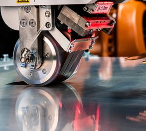

Majority of convectional patterning technologies such as nanolithography, nanoimprint, and micro/nanoprinting are not applicable to aerogel-type nanostructures, like freestanding carbon nanotube (CNT) sheets and highly aligned CNT forests. Previous research showed the use of a laser beam for patterning freestanding CNT sheets and CNT forests strongly depends on optical absorption and requires a tunable lens system for beam focusing. In essence, a laser beam does not provide capabilities for precise variable-depth profile patterning. Another concern for laser cutting is the width of the removed material (the kerf) and the extent of the heat-affected zone. In fact, Raman spectroscopy and analyses of mechanical properties of cut edges show that laser-induced damage spreads deep into laser patterned materials. Recent research has showed that dry plasma etching in a mixture of Ar (He) and O2 can routinely be used for layer-by-layer processing of CNT arrays. Nevertheless, the non-selective nature of plasma treatment limits its application for patterning.
In general, despite there being many available theoretical models and commercially available tools, the material removal mechanism for most of these techniques is not yet deeply understood. Moreover, the patterning of microns thick, freestanding aerogel films and very fragile 3D sponge and foam nanostructures is very challenging, and needs more precise and delicate approaches. Therefore, to facilitate the application of these materials for electronic and optical devices, it is essential to develop techniques for shaping freestanding 2D and 3D nanostructures that result in minimal loss of material, low contamination, and pattern precision on the nanoscale. In this regard, two nanomaterials experts from the University of Texas: Professor Ali Aliev and Professor Ray Baughman, developed a new innovative method for non-contact processing of conductive, nanostructured, low-dimensional materials using field enhanced electron emission. Their work is currently published in the research journal, Nanotechnology.
Their goal was to develop a method that could be deployed for patterning freestanding and supported 2D films, such as highly aligned or randomly deposited CNT sheets, graphene and MXene films, and their composites. To realize this, the authors proposed a self-terminating pulsed electron-emission decomposition technique to pattern CNT aerogel sheets in air. The method was then subjected to tests by being applied to pattern sheets and films of two-dimensional (2D) materials, like graphene and MXene, and to create complex patterns and void elements in three-dimensional (3D) structures, like CVD grown CNT forests, graphene and graphene-oxide/CNT nanocomposite sponges.
The authors reported that their technique exploited self-generated electron-emission pulses (~20 ns) in air. In actual fact, by using the advantages of field enhancement at sharp ends of nanostructured materials, the discharge voltage was reduced to 25–30 V, depending upon the materials density. Further, the method was noted to cause largely non-oxidative sequential decomposition of nanostructure elements neighboring the tungsten tip. The researchers further reported that the main decomposition mechanism was thermal dissociation facilitated by Joule heating and electrostatic removal of debris.
In summary, the study by Professor Aliev and Professor Baughman reported the successful development of a dry-state patterning technique for freestanding or supported nanostructures. The patterning method employed here used a non-contacting sharp W-tip that moves along the surface of the targeted conductive nanostructure. The trade off in the presented approach is that a negative tip causes resistive overheating of cut edges, which in return enhances the heat-effected zone, thereby causing pitting of the W-tip. In a statement to Advances in Engineering, the authors explained the proposed electron emission patterning for processing of carbon and other conductive two- and three-dimensional nanostructures in air could be useful for integration of conductive electronic and optical devices into existing silicon planar technologies. Moreover, by using their technique, multi-electrode sensors, metamaterials, photonic crystals and various electronic components had been successfully fabricated. The innovative method invented by Professor Aliev and Professor Baughman is now under provisional Patent Application #20016P1, Dec.8, 2020 “A method and device for patterning nanomaterials”.


Ali E. Aliev is a Research Professor in Alan G. MacDiarmid Nanotech Institute at University of Texas at Dallas. He graduated National University of Radio-Electronics, Kharkov, Ukraine, received his PhD in Molecular and Thermal Physics and Doctor of Science in Solid State Physics from Academy of Sciences of former USSR. Before joining University of Texas at Dallas he was a head of Advanced Materials Research Department at Heat Physics Institute, Academy of Sciences of Uzbekistan (1992-1998), an invited researcher at LG-Electronics, Seoul (1998-2002). His research activities involve phonon and electron transport in low-dimensional nanostructures, superconductivity in metal oxides, and thermoacoustics.
E-mail: [email protected]
Phone: +1 972-883-6543
Web page: https://en.wikipedia.org/wiki/Ali_Aliev_(physicist)

Ray Baughman became the Robert A. Welch Professor of Chemistry and Director of the NanoTech Institute at the University of Texas in Dallas in August 2001, after 31 years in industry. He is a member of the National Academy of Engineering, the Academy of Medicine, Engineering and Science of Texas, Academia Europaea, and the European Academy of Sciences and Arts; a foreign member of the European Academy of Sciences; a Fellow of the Royal Society of Chemistry, the National Academy of Inventors, the American Physical Society, and the American Association for the Advancement of Science; an Academician of The Russian Academy of Natural Sciences; and is on editorial or advisory boards of Science and other journals. Ray has 102 issued US patents, over 470 refereed publications, over 72,800 citations, and a Google Scholar H-index of 117.
E-mail: [email protected]
Phone +1 972-883-6538
Reference
Ali E. Aliev, Ray H. Baughman. Shaping nanomaterials by short electrical pulses. Nanotechnology; volume 31 (2020) 365302 (12pp)